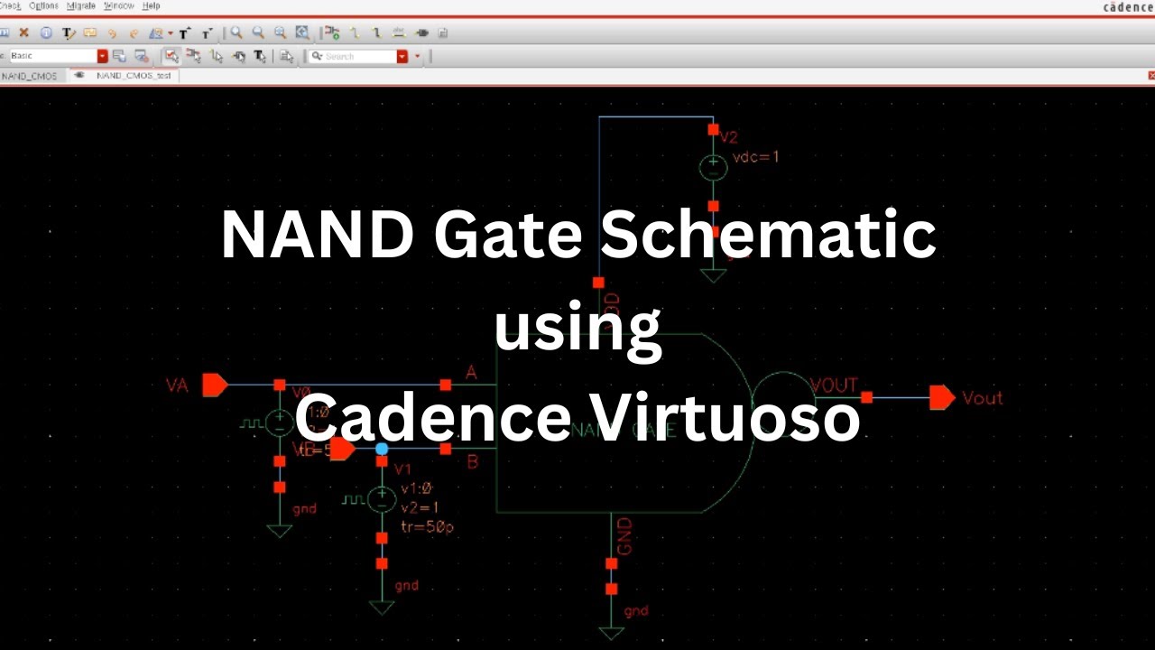
[diagram] circuit diagram nand gate Solution: layout of nand gate in cadence Lab 1 part a procedure: designing and simulating a nand gate schematic
Nor Gate Schematic In Cadence
Nand gate layout input draw lw
Problemas de lvs de compuerta nand en cadence virtuoso
Nand gate circuit and simulation in cadenceNand gate schematic using cadence virtuoso Tutorial #1: drawing transistor-level schematic with cadence virtuosoHow to draw 2 input nand gate layout in microwind.
Layout cadence nand gate virtuoso fig481: a 2-input nand gate layout designed in cadence virtuoso. Tutorial virtuoso cadence layout inverter nand gate cmos pdf basic softwareIntroduction to logic gates.

Ee4321-vlsi circuits : cadence' virtuoso ultrasim vector file simulation
Cadence tutorial -cmos nand gate schematic, layout design and physicalNand gate Nand schematic logic lab6 jbaker courses f16 ee421l cmosedu studentsSchematic and layout of 1x 2-input nand gates with (a) glb applied to.
Schematic transistor level nand gate cadence virtuoso full tutorial cell figure nameNand input schematic gates glb 1x Layout of nand gate in cadence virtuoso . drc and lvs checkNand lab5 verification hierarchical inverter toolbar.
Layout nor cadence gate lab6
Nand gate schematic in cadence1: a 2-input nand gate layout designed in cadence virtuoso. Cadence tutorialCadence virtuoso:: design of nand gate schematic || part-1..
Nand input virtuoso cadence designedNand gate nmos logic transistor schematic using digital universal its ic schematics symbols two given below Nand gate schematic in cadenceNand gate schematic in cadence.

[diagram] circuit diagram nand gate
Cadence virtuoso tutorial: cmos nand gate schematic symbol and layoutCadence gate schematic layout nand cmos assura verification Logic nand gate working principle & circuit diagramNand virtuoso cadence cmos.
Nand gate cadence virtuoso buffer vlsi simulation tb inverters benchNor gate schematic in cadence Ece429 lab5A standard digital cmos nand3 gate and its internal transistor.

Two input nand gate schematic.
Cadence virtuoso layout from schematic[diagram] circuit diagram nand gate Nand gate schematic in cadenceGate nand cadence simulation.
.